









Sparkfun Teensy 4.1, Lockable
Description
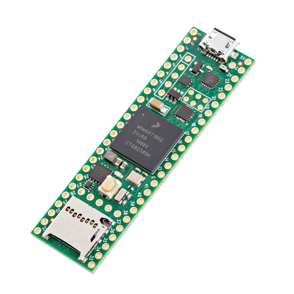
This lockable version is tailored for developers transitioning from prototype to secure final products. It enables write access to the chip's eFuses, allowing permanent locking of the device in a secure mode. By programming an encryption key, your application code becomes encrypted, safeguarding against unauthorized access, cloning, or modification. In secure mode, the JTAG debug port is disabled, ensuring that only encrypted code runs on the microcontroller.
At the core of the Teensy 4.1 is the NXP MIMXRT1062DVJ6B, a crossover MCU that bridges the gap between microcontrollers and high-performance application processors. It features a dual-issue superscalar processor capable of executing two instructions per clock cycle. This efficiency is enhanced by branch prediction, which reduces overhead in loops, and a hardware FPU that accelerates both 32-bit and 64-bit math operations.
The Teensy 4.1's advanced memory architecture includes Tightly Coupled Memory (TCM) for ultra-fast access, ensuring the CPU operates at peak performance. The board also provides options for expanding memory with up to 16MB of PSRAM or a QSPI flash chip, catering to even larger applications.
This microcontroller is designed for efficiency, consuming around 100mA at 600 MHz. It supports dynamic clock scaling, allowing speed adjustments without disrupting serial baud rates or timing functions. Additionally, it features a power on/off pin for low-power projects and RTC support for timekeeping during power-off. For those seeking extra performance, overclocking beyond 600 MHz is possible.
With its robust processing capabilities, expanded memory, and crucial peripherals, the Teensy 4.1 is the ideal platform for high-performance, connected projects demanding maximum efficiency and security.
Properties

Delivered in 5 to 7 days
 Sparkfun Teensy 4.1, Lockable Delivered in 5 to 7 days € 48,20
 Customer questions
Customer Reviews
- Reduced In stock -49 % Sparkfun LED - Ultraviolet € 2,15 € 1,10 View product
- Reduced In stock -50 % Sparkfun Diffused LED - Yellow 10mm € 1,10 € 0,55 View product
- Reduced In stock -50 % Sparkfun Screw Terminals 5mm Pitch (2-Pin) € 1,60 € 0,80 View product
- Reduced In stock -50 % Sparkfun 555 Timer € 1,50 € 0,75 View product
- Reduced In stock -50 % Sparkfun Battery Holder 2xAA with Cover and Switch € 2,50 € 1,25 View product
- Reduced In stock -50 % Sparkfun Diode Rectifier - 1A, 50V (1N4001) € 0,40 € 0,20 View product
- Deal In stock -58 % Sparkfun Rocker Switch - SPST (right-angle) € 3,95 € 1,65 View product
- Reduced In stock -50 % Sparkfun Solder Leaded - 15-gram Tube € 5,65 € 2,85 View product
- Reduced In stock -50 % Sparkfun Coin Cell Battery Holder - 20mm (PTH) € 2,50 € 1,25 View product
- Reduced In stock -49 % Sparkfun Reed Switch € 3,25 € 1,65 View product
- Reduced In stock -50 % Sparkfun Flexible Qwiic Cable - Breadboard Jumper (4-pin) € 3,60 € 1,80 View product
- Reduced In stock -48 % Sparkfun Screw Terminals 5mm Pitch (3-Pin) € 1,65 € 0,85 View product
- Reduced In stock -50 % Sparkfun Barrel Jack Power Switch - M-F (3") € 5,- € 2,50 View product
- Reduced In stock -50 % Sparkfun Female Headers € 2,80 € 1,40 View product
- Reduced In stock -50 % SparkFun Voltage-Level Translator Breakout - TXB0104 € 8,50 € 4,25 View product
Recently viewed items